Posts

Showing posts with the label Open8

Generating 16k ROM using Xilinx IP COREGEN and simulating it in modelsim

The instruction ROM is an IP Core. so before interfacing with the open8, it has to be generated. The method of generating and simulating a ROM Xilinx IP Core is described here. FIND ALL THE FILES HERE 1. app.coe (the initialization file) 2. rom_16k_core.vhd 3. rom_16k_core.vho 4. rom_16k_core.xco 5. top_level.vhd 6. do_memgen.do Creation of the ROM Xilinx 10.1 1. open ISE 2. create a new project 3. tools -> core generator(12.1) (or right click on the device and add a new file 10.1) 4. In the IP catalog -> Memory and storage elements -> RAM and ROM 5. double click on block memory generator, A new window opens 6. In the new window select single port ROM click next, Write first mode 7. Select Read Width = 8 and Read Depth = 16384 for 16K ROM -> next 8. The output ports are unregistered, load initialization COE if required -> next 9. No need to use the Reset pin -> next 10. Generate. (takes a little time then shows successfully generated) This...
BUG in open8 - solved - It is not a bug but a misunderstanding, THANK YOU Mr. SETH HENRY

Image
Hi, There was a misunderstanding regarding to the bug I had encountered while using open 8 core. The bug is that there was a displacement of 1 cycle in the processor code while fetching the return address executing the "RTI" instruction. It is described in detail here . This is not actually a bug because the processor was pipelined in such a way that the data was to be read from the memory in a span of 2 cycles while my assumption about the memory model was that data was fetched in 1 cycle. This pipelining was done in order to increase the frequency of operation. So the memory model is described as follows - 16 k single ported ROM in the write first mode. width = 8 and depth = 16k (16384). The pipeline operation is described here as a stand alone project. (not connected to the open8) library ieee; use ieee.std_logic_1164.all; use ieee.std_logic_unsigned.all; use ieee.std_logic_arith.all; entity rom_16k is port(   Clock             ...

SOC Encounter for layout generation

Image
The netlist for the interfaced design is available. This is to be ported into SOC encounter to generate a layout. Design methodology – top down The design is synthesized so as to define the components in standard cells of the OSU 25 library. This synthesized netlist is imported to encounter to generate the layout. The Steps for chip planning in Encounter are 1.Import netlist 2.Floor plan 3.Create a black box partition of the memory 4.Power planning 5.specify modules and black boxes position on the chip 6.special route 7.Run placement 8.Assign pins for the black box 9.Run trial route – analyze for congestion 10.Run nano route 1. IMPORT NETLIST     The synthesized netlist is imported into encounter and the osu25_stdcells.lef and osu25_stdcells.tlf libraries are mapped. The power nets and ground nets are specified to be “vdd” and “gnd”. 2. FLOOR  PLANNING The sizes of the individual modules were measured for a total utilization of 70%. A memory gen...

Interfaced Design

Image
This post is about interfacing all the modules of the obstacle avoidance project and optimization techniques. The design is inter connected in the HDL description itself. The memory is defined as a black box. A black box in VHDL is an entity without an architecture. Since the memory is to be added later, it is described as a black box. The VHDL files for the interfaced design is sourced into the RTL compiler. As you can see, a lock to the side of the memory module. This shows that the memory is a black box. The netlist is generated for this design using RTL Compiler. The next step is verification of this netlist. But since the memory is not available, it cannot be tested. DESIRED FREQUENCY OF OPERATION The desired frequency of operation was set to 0.5 GHz (2000 ps). The clock was set to this requency using the set clock command of RTL compiler. The worst negative slack is calculated.  It is seen that for a frequency of 0.5 GHz, the worst negative slack is -1406 ps and henc...

MOTOR CONTROLLER TO OPEN8 INTERRUPT INTERFACE

Image
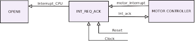
The Interrupt from the motor controller to the CPU needs to be high for 1 clock cycle. There is not interrupt acknowledge signal from the Open8 CPU that can turn off the interrupt after 1 clock signal. If the motor controller interrupt is more than one clock cycle, The CPU interprets it as a separate request. So there is a need for a moderator that  Receives an interrupt request from the motor controller Responds to the interrupt by sending a signal to the CPU interrupt line which is high for exactly one clock cycle.  After sending the interrupt request to the CPU, sends an interrupt acknowledge signal to the motor controller.  This moderator is Int_req_ack module. The Int_req_ack module has a 2 bit counter which is initialized to “00”.  When the motor interrupt goes high, the counter is incremented by 1 every clock cycle and the interrupt_CPU line goes high. Since we need the interrupt_CPU line to be high for exactly one clock signal, the counter is rese...

MOTOR CONTROLLER

Image
The motor controller is the interface to the stepper motor. Stepper motor has four coils. The coils of the stepper motor are to be energized as follows for it to rotate forward. Stepper motor operation So to rotate the stepper motor in the “forward direction”, the sequence 1100 is to be right shifted by one bit for each step. A step is defined as the linear distance traveled when the sequence is shifted right by one bit. To rotate the stepper motor in the “reverse direction”, the sequence 1100 is to be shifted left by one bit for each step. Thus the operation involving rotation of the stepper motor is shifting the sequence 1100 right or left onto the coils of the stepper motor. An encoder provides feedback upon completion of one step rotation. The feedback signal is used as an indicator to shift the next pattern in. Step Angle: There are 4 steps in 360 degrees. Hence the step angle is 90 degrees step angle = 360/4 = 90 if the diameter of the wheel is 5 cm, the distance ...

Modification of OPEN8 core to interface with the Memory

Image
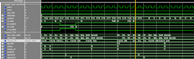
The open8 core is to be modified to interface with the memory. The modification is described here. REFERENCE TO THE OPEN8 INSTRUCTION SET GUIDE Description : There is an implementation change to the open8 core so as to interface it with the memory provided with us. The implementation change is for instructions RTI (return from interrupt) and RTS(return from subroutine). BUG 1. The interrupt occurs 2. There are 3 bytes that are stored in the stack The PSR and the 16 bit memory return address. They are stored in memory locations 127, 126, 125. This is with accordance with the Instruction set guide. 3. After stack operations is done, it  jumps to the ISR. ISR is pointed to location pointed to in memory by 129,128 as specified in the Assembly language reference manual. 4. In the ISR, it continues to execute code and when I use the RTI instruction, the control does not resume execution from where it left off. Instead it starts executing form location 0. 5. When RTI is executed...

INTERFACE BETWEEN Open8 and MEM

Image
A 256 byte memory model is described in VHDL to using on chip BRAM for testing on FPGA board. It is interfaced with the Open8 soft processor. It is used as both program memory and data memory. The program can be loaded in binary into the memory, interfaced with open8 and can be simulated using modelsim. 1. Using the BRAM in the FPGA board as program memory/Data memory. Memory Size open8 has 16 bit address lines. I have implemented a 256 byte RAM (Uses the internal BRAM of the spartan3 FPGA) to connect it to the FPGA. The memory entity is described below ----------------------------------------------------------------------------- -- Memory: RAM -- Desc: Instruction/ data memory -- no of entries : 256 bytes -- no of bits    : 8 -- we - write enable -- re - read enable -- en - select memory -- addr - address(8 bits) -- di - data in  (8 bits) -- do - data out (8 bits) ------------------------------------------------------------------------------ entit...

Layer 0 - obstacle avoidance of SUBSUMPTION Architecture

Image
PROJECT : It was required to build a system on chip using the following components 1.An open core from www.opencores.org 2.A custom block implementing a functionality 3.A memory which is generated by a memory generator built by professor Garrett Rose. I read through different topics but my interest in robotics kicked in when I read a paper on subsumption architecture described in the paper “A Robust Control System for Mobile Robots” by the famous H.A. Brooks from the AI lab at MIT. INTRODUCTION Subsumption architecture is a layered architecture for building control systems for robots. The  control system is composed of number of individual layers. Each layer performs a function independent  of the other layers. For example consider a robot composed of the following layers Layer 0: Obstacle avoidance Layer 1: Wandering Layer 2: moving towards an object of interest Layer 0 is the lower most layer, There is a processor just for this layer that receives input from the se...